
Plasma Etching

Oxford NGP80 RIE
Staff Contact: Erik Vick
Location: High Bay
Gases: CF4, CHF3, C2F6, SF6, Ar, O2
Standard Etches : SiO2, Si3N4, Glass, Si, and SiC
Samples : 1 – 4″ Wafer or Equivalent Area
Allowed Masking Materials: Photoresists and SU8
Etch rates, selectivity to photo-resist, uniformity and wall angle profile data:
A standard process for Si etching (Fluorine based) is checked weekly and data is
collected to observe and correct deviations >10%. Chamber cleaning, process
conditioning steps and MFC’s calibration are scheduled based on the data to
maintain equipment performance.
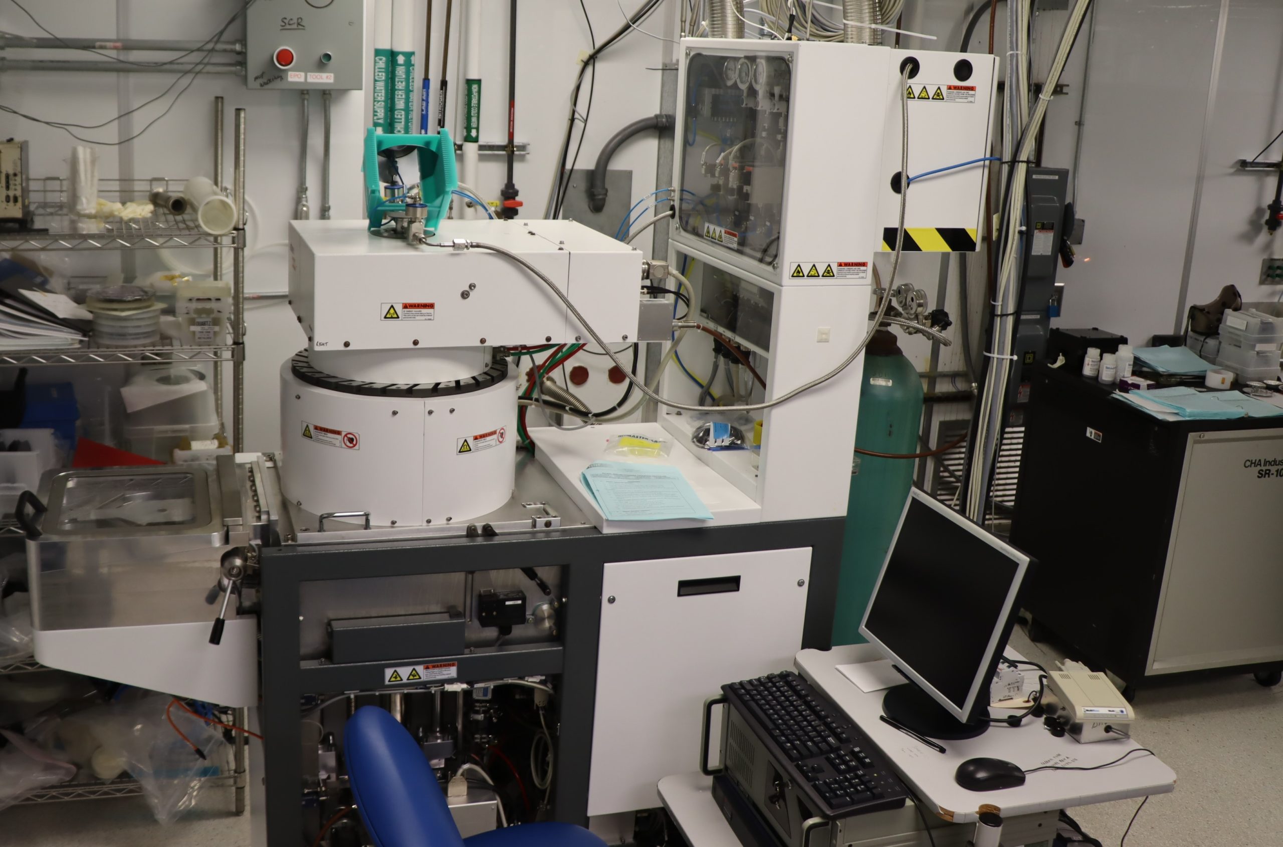
Alcatel Deep Reactive Ion Etch
Staff Contact: Erik Vick
Location: High Bay
Gases : SF6, C4F8, CF4, Ar, O2
Standard Etches : Si, Glass, SiO2
Samples : 1 – 6″ Wafer or Equivalent Area
Allowed Masking Materials : Photoresist, SU8, and Nickel

Oxford Plasmalab 100 ICP Etcher
Staff Contact: Erik Vick
Location: High Bay
Gases : BCl3, Cl2, SF6, O2, Ar, N2
Standard Etches : GaN, AlGaN
Samples : 1 – 6″ Wafer or Equivalent Area
Allowed Masking Materials : Photoresist and SU8
Etch rates, selectivity to photo-resist, uniformity and wall angle profile data:
A standard process for Si etching (Chlorine based) is checked weekly and data is
collected to observe and correct deviations >10%. Chamber cleaning, process
conditioning steps and MFC’s calibration are scheduled based on the data to
maintain equipment performance.
Oxford Plasmalab 100 Cobra Etcher
Staff Contact: Erik Vick
Location: Plasma Bay
Gases :
Standard Etches :
Samples :
Allowed Masking Materials :

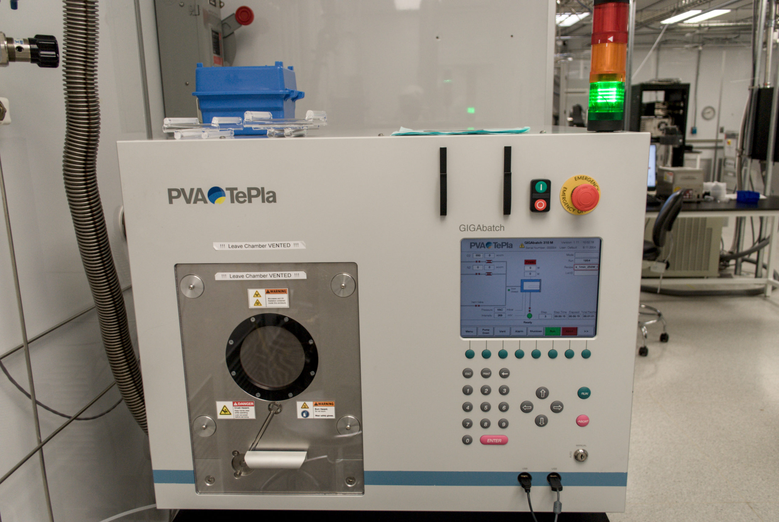
TEPLA Plasma Asher
Staff Contact: Erik Vick
Location: Plasma Bay
Gases : N2, O2
Standard Etches :
Samples :
MARCH Plasma Asher
Staff Contact: Erik Vick
Location: Plasma Bay
Gases : O2
Standard Etches :
Samples :
