Metrology

Dektak XT Contact Profilometer
Staff Contact : Elena Kovalik
Location: PECVD Bay (205)
Tip Radius : 12.5um
Samples : Pieces – 8″ Wafer
Vertical Repeatability: 4 Angstroms on 0.1 micron step
Max Scan length: 55 mm
Nanometrics
Staff Contact : Elena Kovalik
Location: Plasma Bay (207)
117 Vac
±5% Margin of Error
50/60 Hz


Woollam M2000 Ellipsometer
Staff Contact : Elena Kovalik
Location: PECVD Bay (205)
Sample- Pieces thru 6″ wafers
Standard and transmission measurements
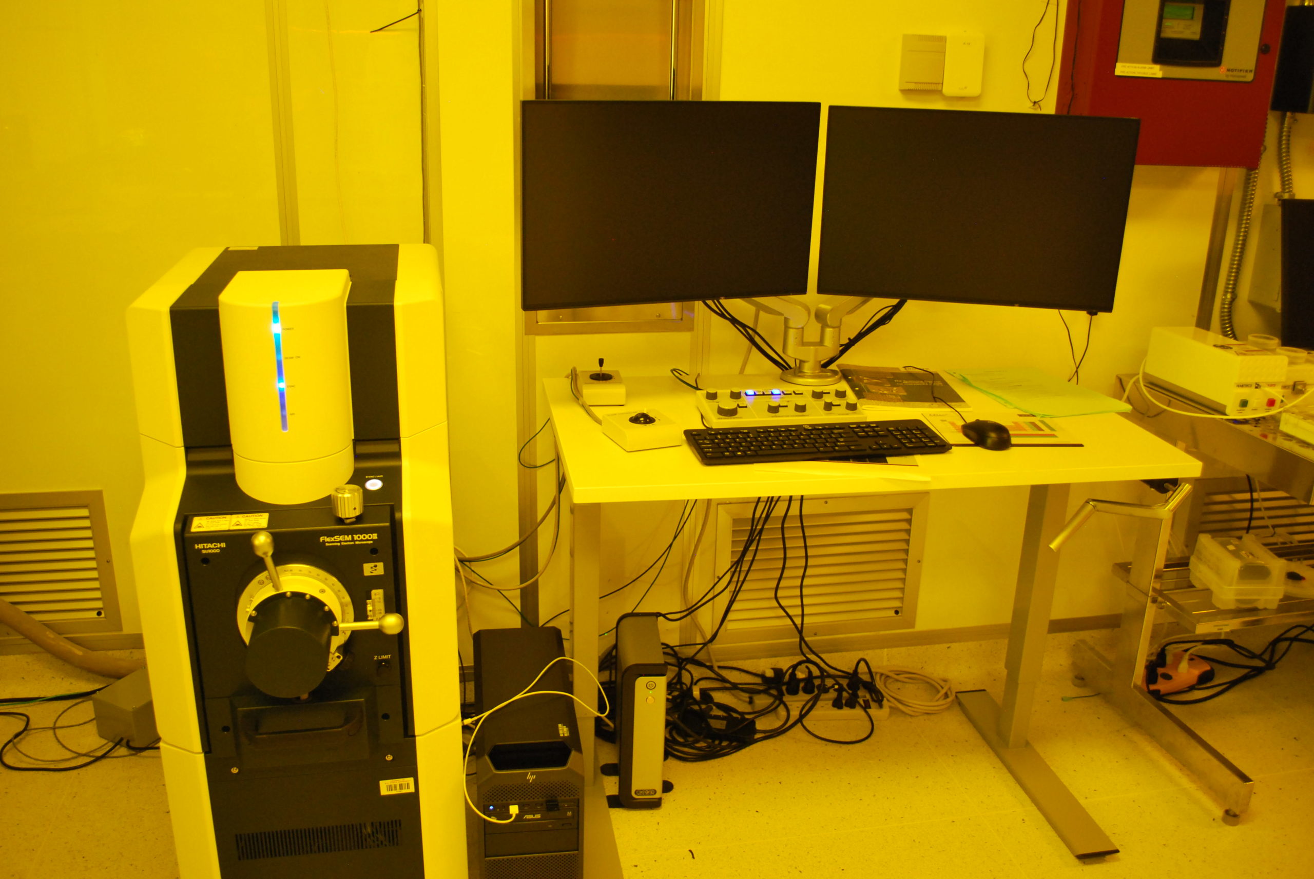
Hitachi SEM
Staff Contact : Elena Kovalik
Location: Stepper Room (211)
Resolution: 4.0 nm at 20kV (high vacuum)
Magnification: 6x-30,000x (photo mode), 16x-800,000x (on display)
Image Data Saving: up to 5120 x 3840 pixels
Elemental Mapping (EDS)
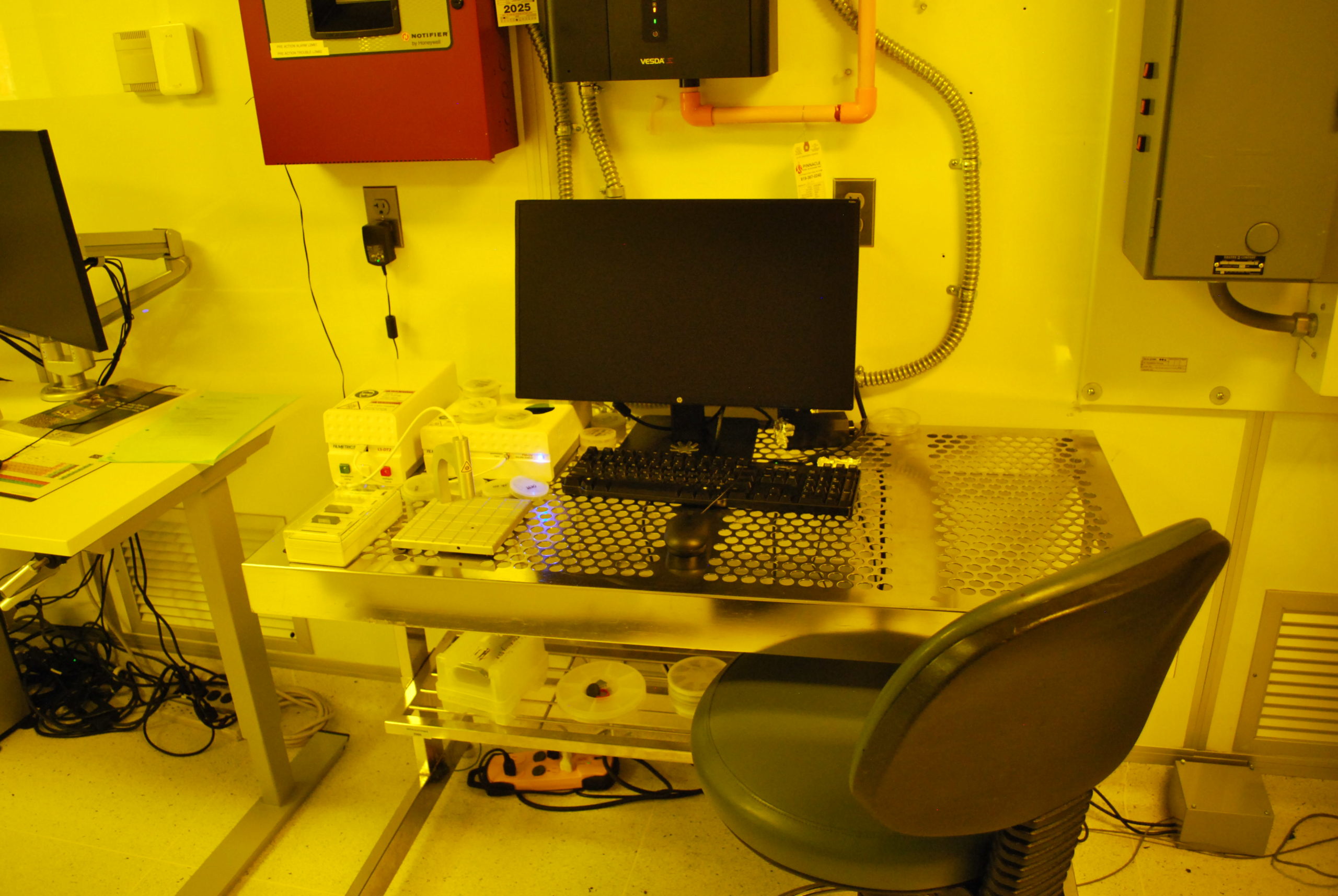
Filmetrics
Staff Contact : Elena Kovalik
Location: Stepper Room (211)
Thickness Range: 1 nm – 40 microns
Wavelength Range: 190-1100 nm
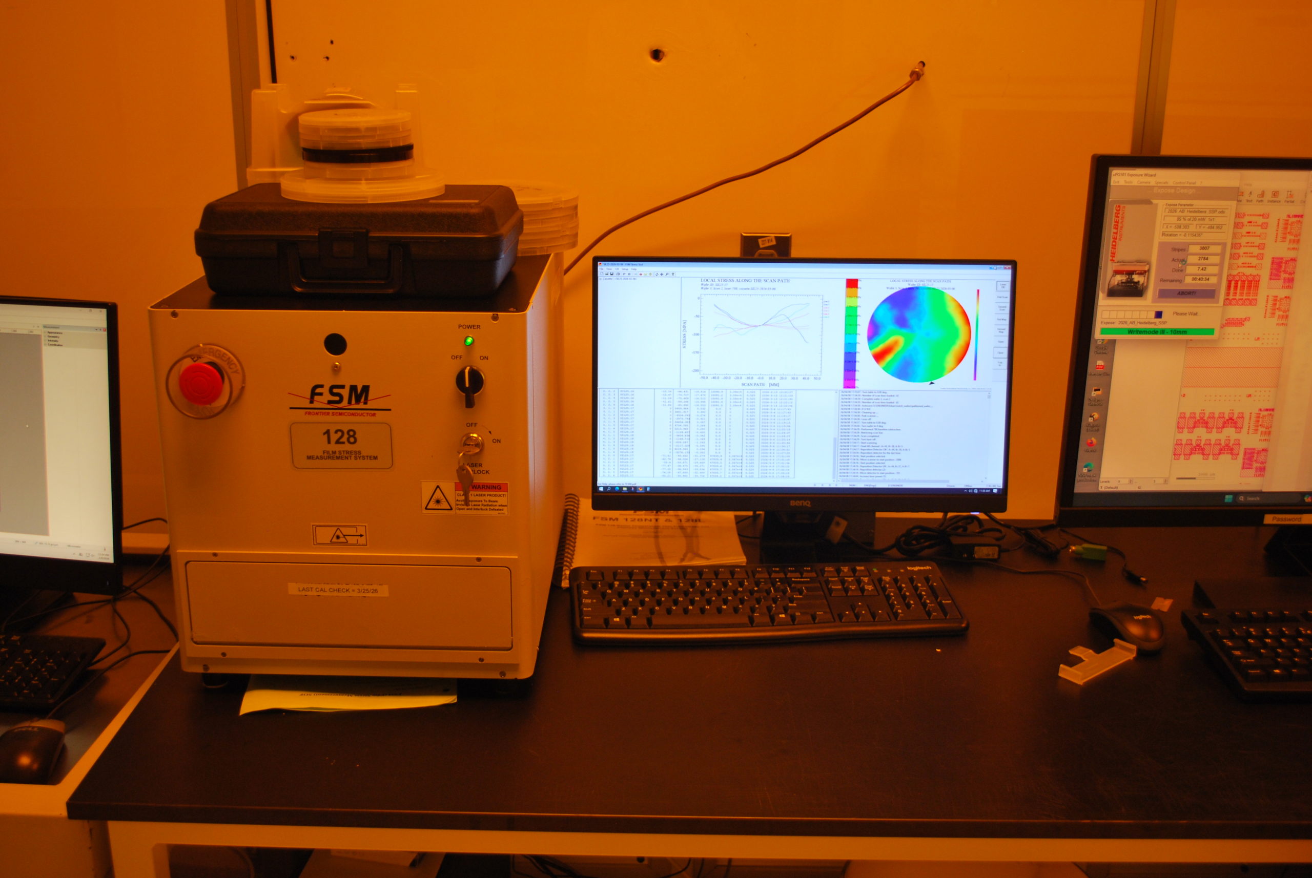
FSM Stress Measurements
Staff Contact : Elena Kovalik
Location: Photo Room – Develop Side (238)
Sample Sizes – Must be full size wafers: 2″, 3″, 4″, 6″
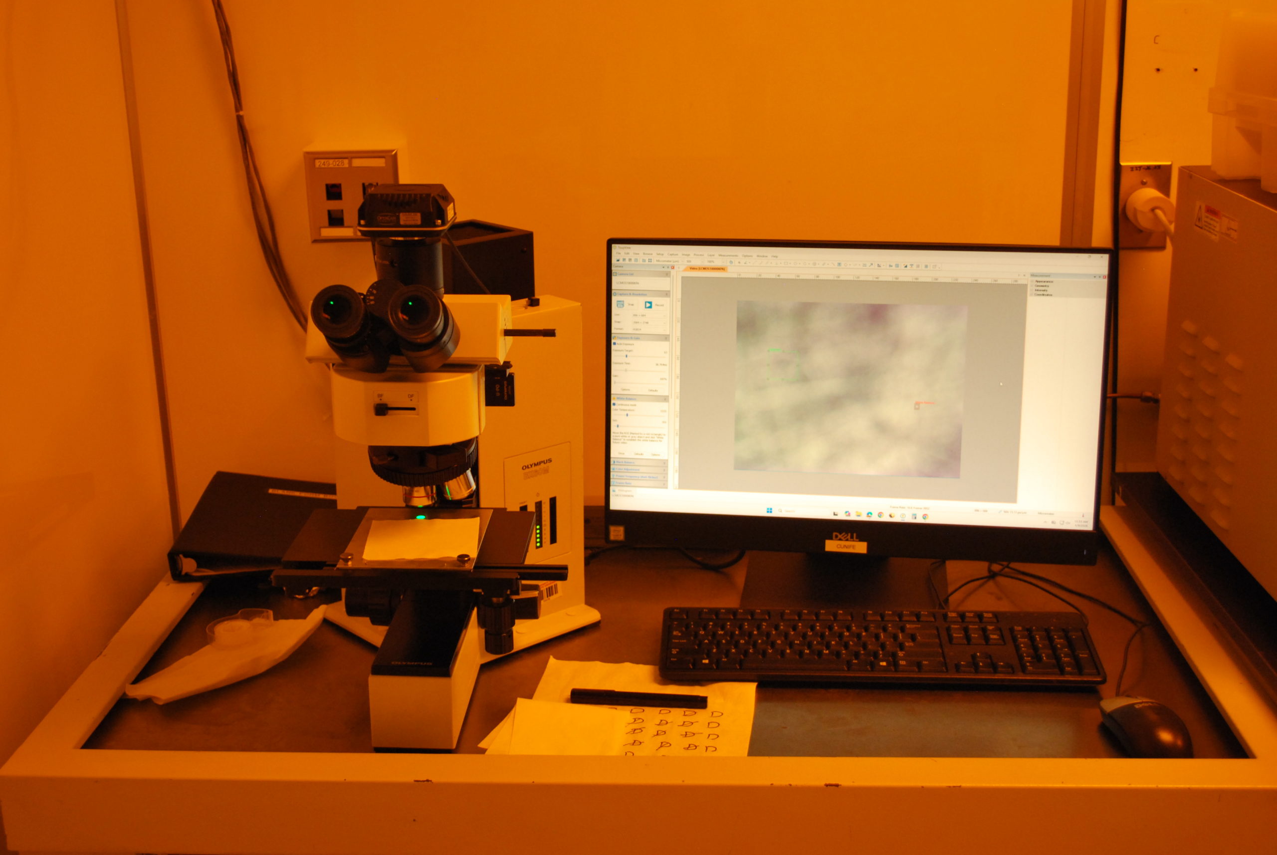
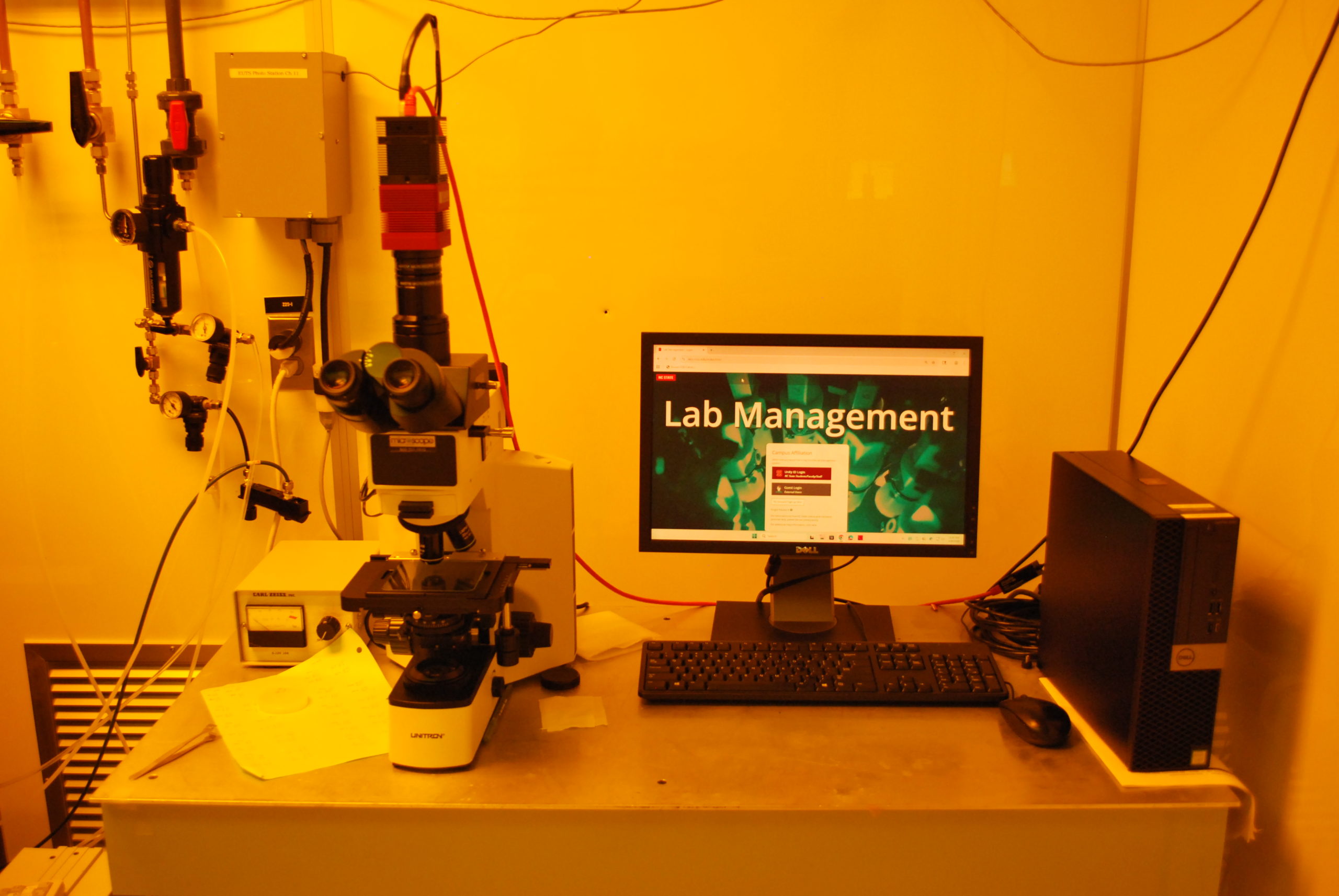
NNF has several optical microscopes with varying capabilities. Pictured are the optical (left) and infrared (right) microscopes located at either side of the photo room.