Lithography
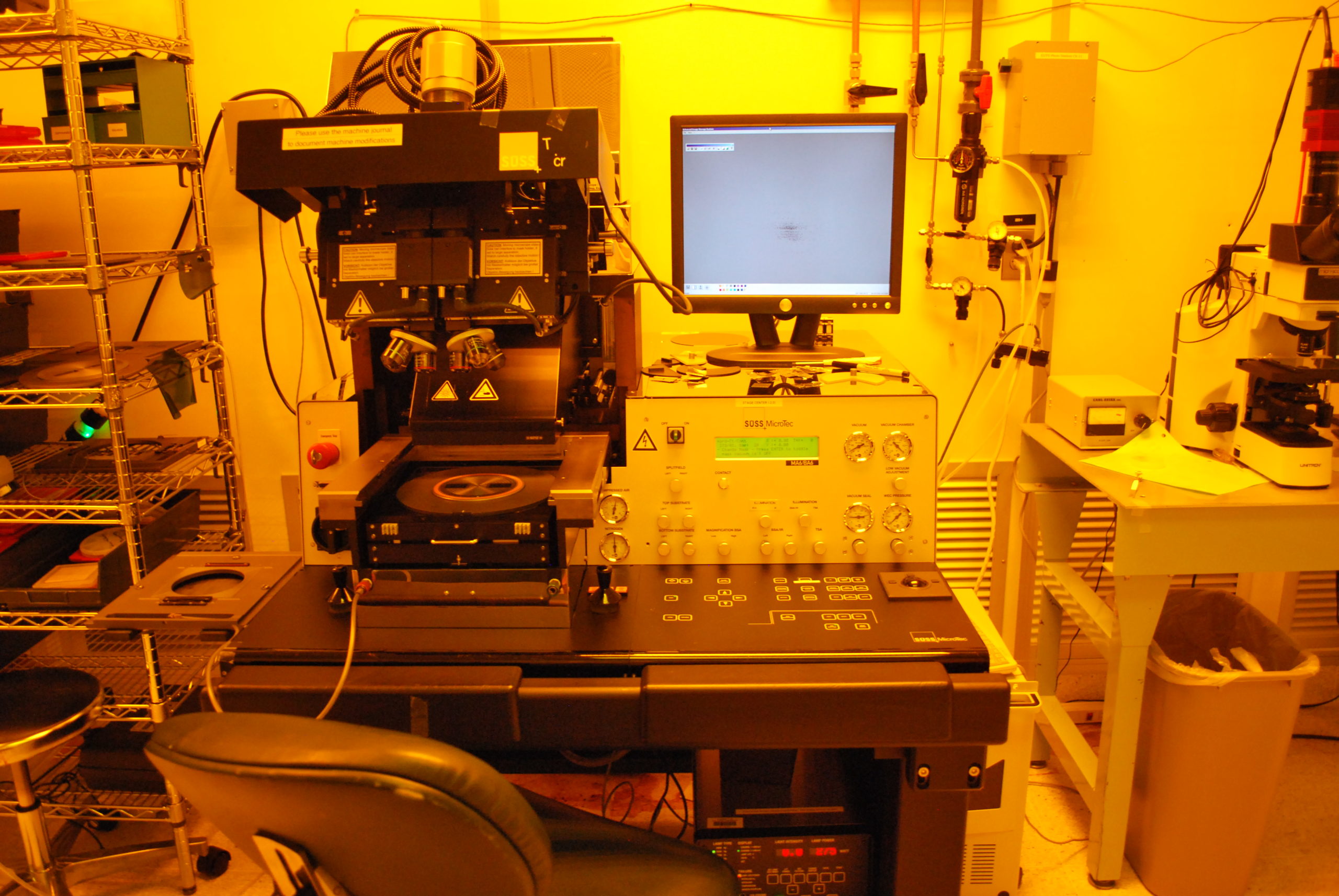
Suss MA6/BA6 Contact Aligner
Staff Contact: Borys Kolasa
Location: Photo Bay – Spin Side
Minimum Feature Sizes: 2um
Samples: 10mm Pieces to 1-6″ Wafer (Thickness 200um to 4mm)
Front Side and Back Side Alignment
Mask Holders: 4″, 5″, and 7″
Sample Holders: Vacuum chuck for pieces up to 3″ wafers, a chuck for 4″ wafers, and a chuck for 6″ wafers.
Exposure Modes: Flood, Proximity, Soft Contact, Hard Contact, and Vacuum Contact.
Exposure calibration checks:
UV energy and uniformity is checked biweekly and adjusted if needed.
We calibrate the lamp output to the i-line (365nm) channel. The i-line intensity is checked to be 10.0 +/- 0.2 mJ/s with a calibrated hand held meter and the power supply is adjusted if needed so the output is accurate. Uniformity is checked and adjusted if needed to be better than 5% across a 4″ area.
*Note, this is a broadband exposure system. We only calibrate the i-line, but the other line intensities track accordingly. The total energy output is closer to 45mW/cm2 if adding all the relevant wavelengths.*
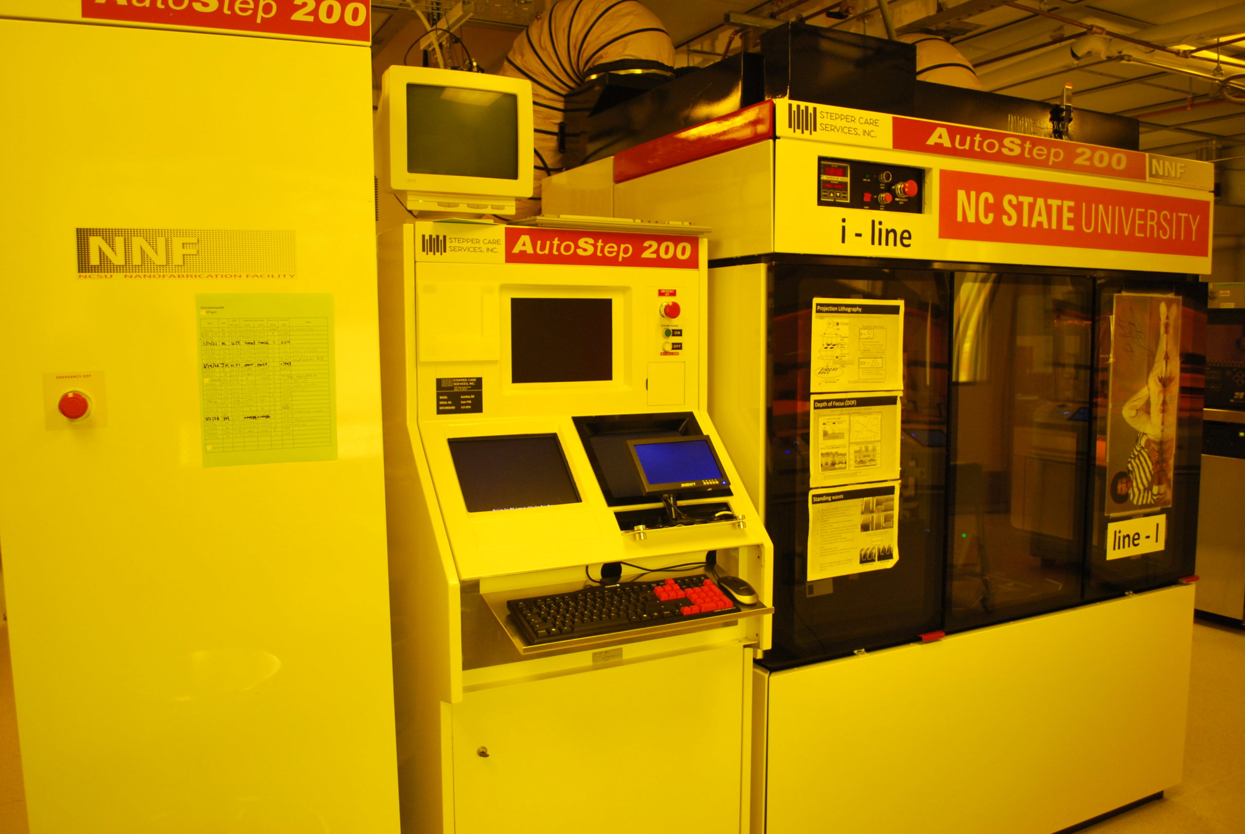
GCA 5X Reduction i-line Stepper
Staff Contact: Borys Kolasa
Location: Stepper Room
Minimum Feature Sizes: 0.6um
Registration better than 500nm
Samples: 10mm Pieces – 6″ Wafer (Sample Thicknesses ranging from 300µm to 1mm)
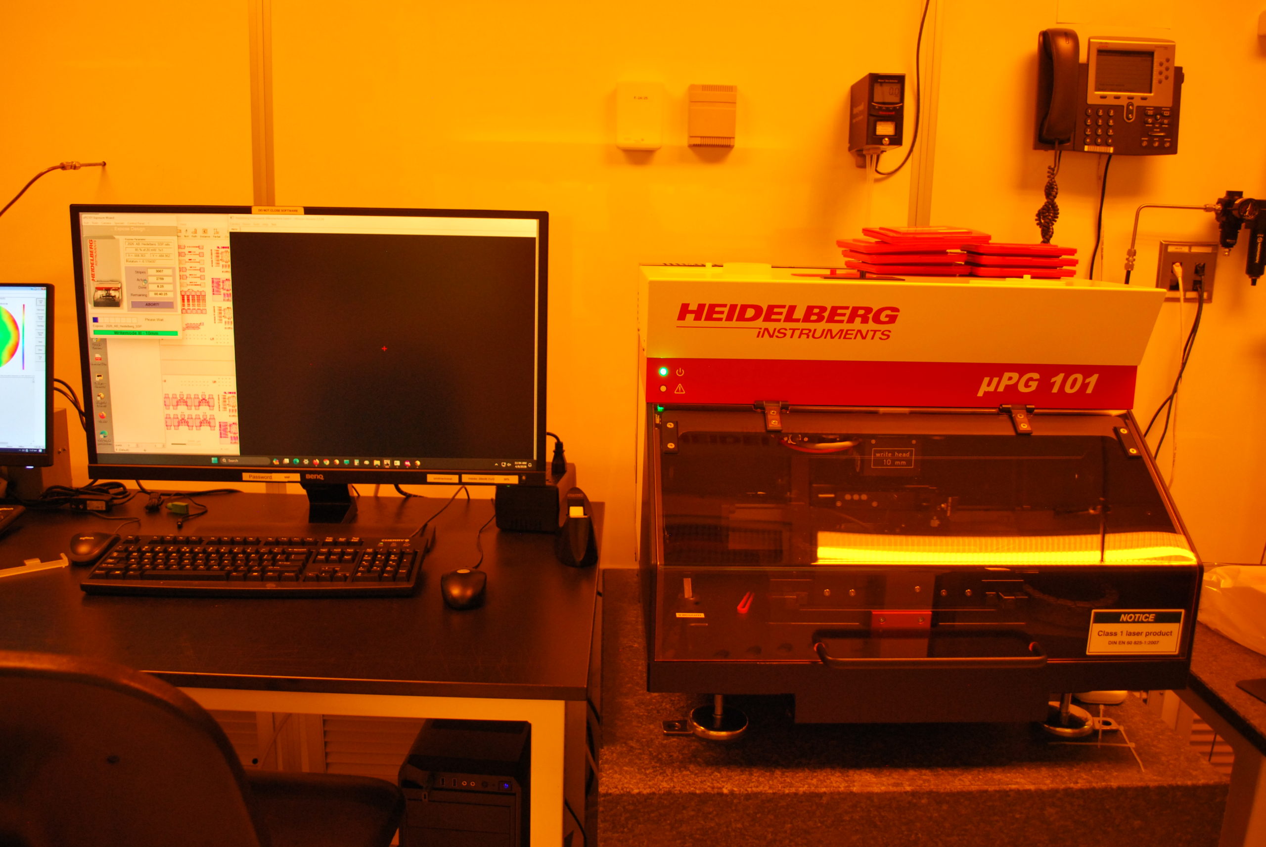
Heidelberg uP-101 Direct Write Lithography
Staff Contact: Borys Kolasa
Location: Photo Room – Develop Side
Minimum Feature Sizes: 0.8um
Samples: Pieces to 6″ x 6″ Sample
375nm UV Diode Laser for Positive and Negative Photoresists including SU8
Mask Writing for MA6 and GCA
Grayscale Exposure Mode 3D Lithography
System calibration checks:
Laser energy and system focus are checked monthly and adjusted if needed.
This baseline process is calibrated for writing photo masks. Commercially purchased, pre-coated blank mask plates are exposed using a dose and focus matrix. The mask plate is then developed, etched and inspected to find the optimum energy and focus. The smallest features are then measured to make sure they are accurate to better than 200nm of the targeted dimensions.
Contact staff for current calibration data.
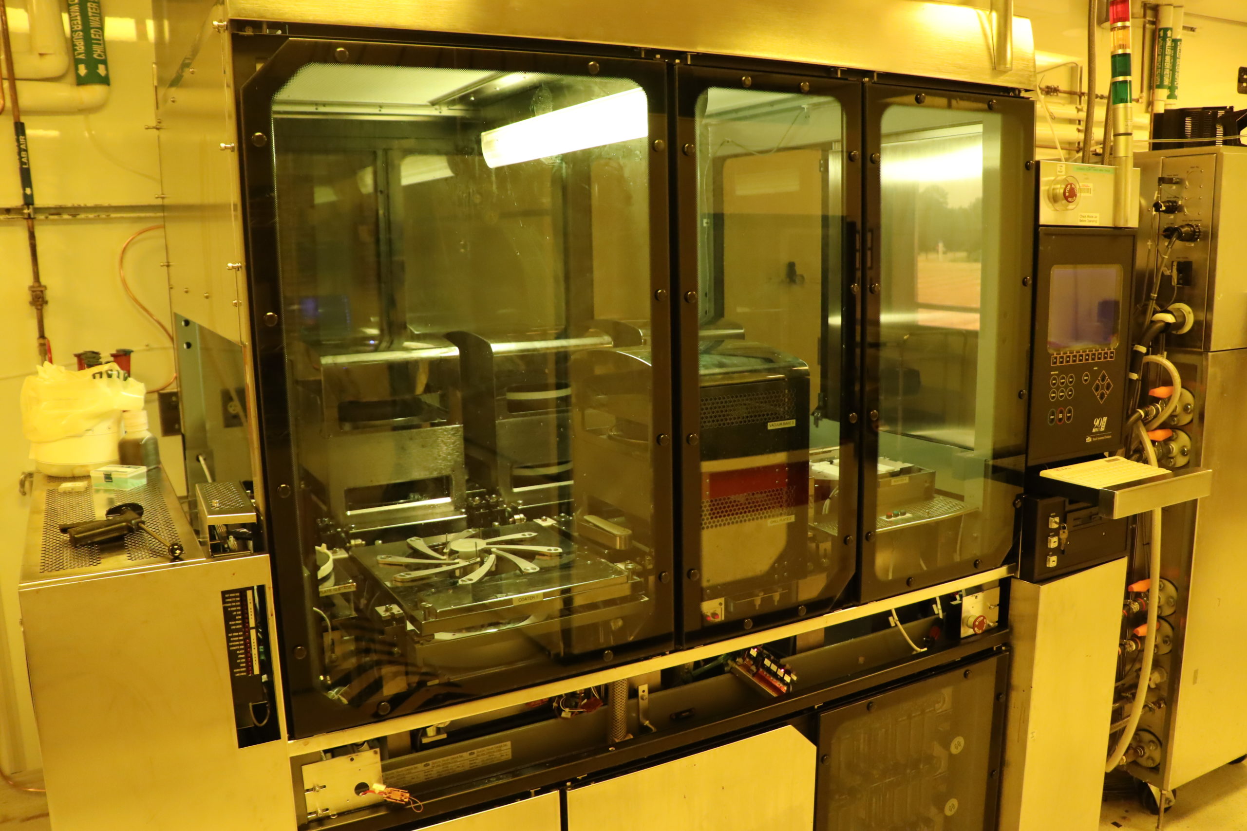
Coat Track
Staff Contact: Borys Kolasa
Location: Stepper Room
Wafer Size: 4″ and 6″
Vacuum Baking
Capable of coating all positive photoresist
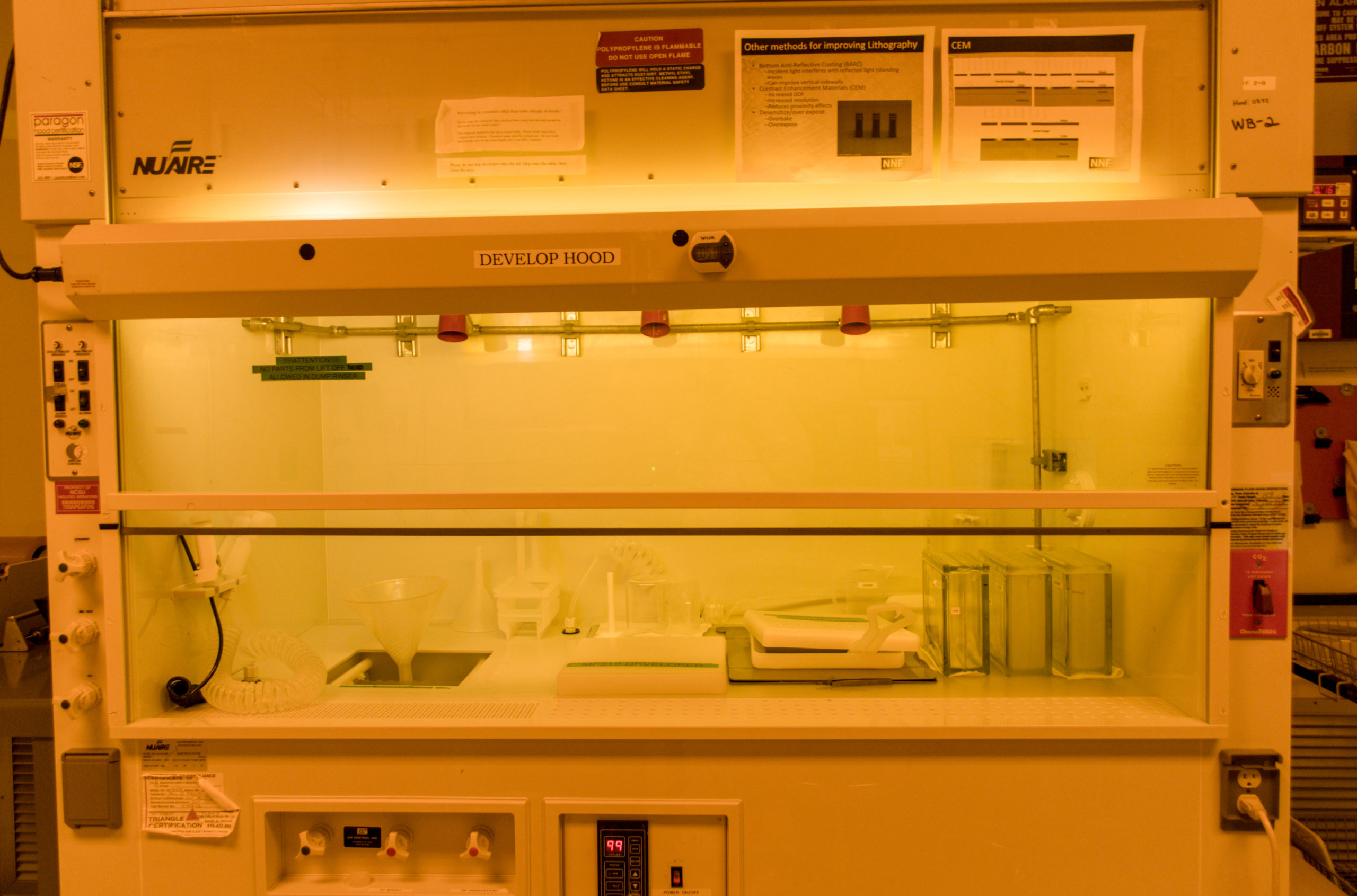
Develop Hood
Staff Contact: Borys Kolasa
Location: Photo Room – Develop Side
In addition to the Cee stations, wafers can be developed manually in the tanks in this hood. Capabilities include:
- MF-319
- CD-26 (MF-300)
- AZ-400K
- SU-8 developer (PGMEA)
- NMP for photoresist stripping
- QDR tank for rinsing